
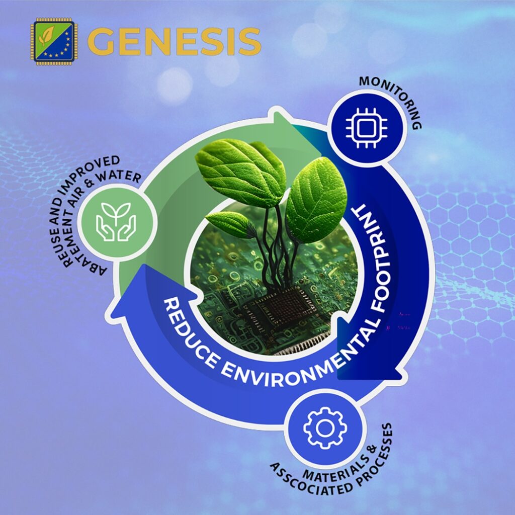
The GENESIS project brings more than 50 European partners together to reduce the environmental impact of semiconductor manufacturing. Fraunhofer IPMS coordinates research on waste and emissions. The work covers alternative process materials and resource recovery from production waste. It addresses a growing challenge as demand for microchips increases. Microelectronics has made major technical progress in recent decades. However, chip manufacturing requires materials, process gases, water and chemical treatments. GENESIS stands for GENerate in Europe a Sustainable Industry for Semiconductors. The project aims to develop technologies that improve sustainability across the semiconductor life cycle.
CEA-Leti coordinates the three-year project. The project is intended to deliver new technologies by 2028. It aligns with the European Green Deal and the EU Chips Act. The consortium includes industry, research and academic partners from across the European semiconductor value chain. Its work focuses on reducing emissions, replacing critical materials and developing recycling methods. Fraunhofer IPMS leads the work package on minimizing waste and emissions. This work package involves 25 project partners. The institute also contributes to other GENESIS activities. It works alongside Fraunhofer ENAS and Fraunhofer EMFT.
Reducing emissions from process gases
A major research area at Fraunhofer IPMS concerns per- and polyfluoroalkyl substances, known as PFAS. The work also covers greenhouse gases used in semiconductor processes. The institute is investigating alternative materials and methods. It is also examining ways to reduce PFAS use. Process gases such as sulfur hexafluoride, SF₆, and nitrogen trifluoride, NF₃, are another focus. These gases have a significantly higher global warming potential than carbon dioxide. Their use is linked to semiconductor manufacturing processes. Therefore, selecting alternatives and controlling emissions can affect the environmental performance of a fabrication process.
Fraunhofer IPMS is evaluating alternative gas mixtures. It is also optimizing existing waste gas cleaning systems. The practical aim is to reduce emissions while considering industrial semiconductor production requirements. Changes to gases, materials or cleaning systems must be assessed under relevant process conditions. Within GENESIS, the waste and emissions work package provides a framework for this research. Partners from across the semiconductor value chain are involved.
Material recovery from CMP slurries
The project also examines the reuse of materials from wafer processing. Fraunhofer IPMS is working with industrial partners to treat and reuse chemical mechanical planarization, or CMP, slurries. These liquid suspensions are used to polish wafers. They contain water, chemicals and extremely fine abrasive particles. CMP is a recurring requirement in semiconductor manufacturing. As a result, its material streams are relevant to efforts to reduce resource consumption and waste. Researchers are investigating how used slurries can be processed. The goal is to recover valuable raw materials and return them to the production cycle.
This approach addresses several issues at once. Reusing suitable material streams can reduce the consumption of new materials. It can also lower water use and limit waste from wafer polishing. Moreover, it creates an opportunity to recover materials that would otherwise leave the process as waste. The work supports GENESIS efforts to reduce dependence on critical raw materials. It also contributes to improved recycling methods in semiconductor production.
Testing sustainable processes in cleanrooms
Fraunhofer IPMS will use its 200- and 300-millimeter cleanrooms to test sustainable semiconductor processes. Industrial partners will participate in testing under realistic conditions. This allows researchers to assess new materials, gas mixtures and waste reduction methods. The tests will show how these approaches affect manufacturing processes before industrial application. For process development, this environment is intended to reduce implementation risks. It may also support the adoption of environmentally focused solutions.
The institute can draw on experience from the BMFTR-funded GreenICT project. GENESIS combines project management, statutory compliance and consolidation with scientific work packages. These work packages cover real-time monitoring and sensors, environmentally friendly materials, reduced dependence on critical raw materials and the minimization of waste and emissions. The project is funded through the European Union’s Chips Joint Undertaking programme. Funding also comes from associated member states and Swiss support for Swiss partners. The Free State of Saxony supports partners based in the region.