
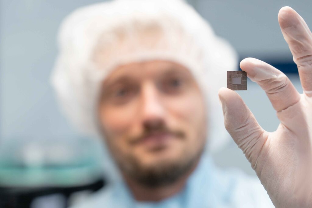
TRUMPF is presenting an ultrashort pulse laser application at Semicon Taiwan. The process produces cooling structures directly within AI chip stacks. It addresses heat dissipation, which is becoming a major constraint in high-performance processors. The process machines microstructures in materials such as silicon carbide and diamond. It is intended to support integrated cooling concepts for advanced semiconductor packaging.
The increasing computing density of AI processors is raising the thermal load inside semiconductor packages. Therefore, manufacturers are moving beyond cooling systems for server racks and data centers. Advanced packaging stacks chips or connects them closely. This approach concentrates more computing power in a smaller space. However, it also brings heat generation closer to critical components. Cooling must therefore be integrated closer to the heat source. Microfluidic cooling and heat spreaders are among the concepts in semiconductor development road maps. Both require extremely fine structures within the chip package. Producing these structures economically and reliably is challenging. This is especially true for hard materials such as silicon carbide.
Integrated cooling moves into the chip stack
Advanced packaging is changing the thermal requirements of semiconductor production. When chips are stacked or positioned close together, conventional external cooling has limited effectiveness. Heat generated inside the package can only be dissipated to a limited extent. As a result, local cooling functions within the chip stack are becoming increasingly relevant. Microfluidic cooling and heat spreaders use fine channels and other structures. These features guide heat away from the areas where it is generated. Their effectiveness depends on the cooling concept and the manufacturing process. Suitable processes must create the required geometries in package materials. Silicon carbide is one suitable material for demanding semiconductor applications. It can also dissipate heat efficiently. However, its hardness makes it difficult to machine using established processes.
The dimensions of the required structures create another challenge. Semiconductor manufacturers need processes that produce small, accurately defined cooling geometries. These processes must also maintain suitable throughput. Surface quality and geometry control must therefore be combined with industrial productivity. TRUMPF’s application is designed to create these structures directly within the chip stack. This allows cooling features to be incorporated into the package.
Ultrashort pulses machine hard materials
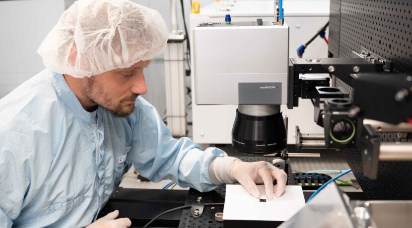
The TRUMPF process uses ultrashort pulse lasers to remove silicon carbide. It forms cooling structures with micrometer-level accuracy. According to the company, industrial suitability depends on several factors. These include high laser power, beam-shaping technology and application expertise. The process can also machine other materials, including diamond. Compared with etching, TRUMPF states that its ultrashort pulse laser process can achieve processing speeds at least five times higher. It can maintain surface quality and accurately defined cooling geometries. This is significant because integrated cooling depends on the geometry of the channels and other microstructures.
Deviations can affect how reliably heat is dissipated within the chip stack. Therefore, manufacturers must assess more than whether integrated cooling structures can be produced. The structures must also meet the quality and cost requirements of industrial production. The laser application presented at Semicon Taiwan addresses this manufacturing challenge. It provides a route for machining fine cooling features in difficult-to-process materials. Moreover, it supports the growing role of thermal management in advanced packaging for future AI chips.