
Fraunhofer IPMS will present semiconductor manufacturing and integration technologies at SEMICON Europa 2026 in Munich. Its work examines how separately manufactured chip components can be combined. It also covers photonics and non-volatile memory. Manufacturers can use this research to assess new device and integration processes under industry-relevant conditions. The institute’s work spans wafer processing, device development and system integration on 200 mm and 300 mm wafers.
A central programme is APECS, a European pilot line being established under the leadership of Research Fab Microelectronics Germany and other European partners. The line forms part of the Chips for Europe Initiative under the EU Chips Act. APECS is intended to provide companies with industry-oriented access to advanced packaging and heterogeneous integration technologies. Its focus is combining chiplets, memory devices, sensors and photonic devices in semiconductor systems. Fraunhofer IPMS contributes wafer processing, integration and system development expertise as a member of the FMD network. The institute will exhibit at SEMICON Europa from November 10 to 13. It will be located at the joint Silicon Saxony booth B1 221 in Hall B1.
Connecting chiplets at wafer level
Fraunhofer IPMS is developing two approaches for combining separately manufactured chip components. In 2.5D integration, chiplets sit side by side on an interposer mounted on a substrate. The interposer provides a high-density interconnection layer. It also creates short electrical connections between the components. This arrangement allows functions such as sensors and memory to be manufactured separately with different technologies. They can still exchange data at a level comparable to a monolithically integrated chip. Computing logic, memory and other functions can therefore be combined in a modular system.
Unlike in 3D integration, the components are not stacked vertically. A second approach is called quasi-monolithic integration. It places chiplets in structured recesses, or pockets, within a silicon wafer. The surface is then planarized and prepared for wafer-level interconnection. Fraunhofer IPMS says it demonstrated this method for the first time within APECS. The approach combines chiplet modularity with the integration density of wafer-based manufacturing. As a result, different components can be brought into a common process.
Silicon nitride platform for photonic circuits
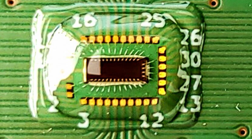
For photonic systems, Fraunhofer IPMS is developing electro-optical devices and CMOS-compatible manufacturing technologies on 200 mm and 300 mm wafers. Its silicon nitride waveguide platform is available on both wafer sizes. It supports wavelengths from the visible spectrum to the mid-infrared region. According to the institute, the platform provides very low optical losses across this range. This allows developers to build complex photonic integrated circuits. Applications include photonic biosensors, photonic computing and quantum technologies. The platform also supports hybrid integration with active components. Electronic and optical functions are integrated at wafer level. This gives developers a common manufacturing platform for devices that combine both functions. It also supports cost-effective production in large volumes. Moreover, the broad wavelength range allows use in different sensing and data-processing applications.
Ferroelectric memory for embedded systems
Fraunhofer IPMS also offers hafnium oxide-based ferroelectric memory technologies through its pilot-line services. These include non-volatile FRAM and FeFET technologies. The institute also provides reference designs for embedded memories and AI accelerator circuits. According to the institute, the devices operate below one volt and switch in the nanosecond range. They retain data without power and are designed for high endurance and reliability.
Fraunhofer IPMS says its ferroelectric layer stacks support device performance and stability under demanding conditions, including elevated temperatures. Potential uses include embedded applications, intelligent sensors and edge-computing systems. These applications require fast processing, low power consumption and permanent data storage in a small space. Current work focuses on improving device concepts and process modules. It also addresses integration into established semiconductor manufacturing processes. External partners can access design kits and platform technologies. They can use these resources to develop their own circuits and test structures. Fraunhofer IPMS supports fabrication and electrical characterization. Therefore, designs can be evaluated for specific applications or demonstrators.