At AKL’26 in Aachen, experts described a laser industry that is no longer defined mainly by individual sources, but by the way lasers are embedded in production, inspection, computing, medicine and energy systems. The practical relevance is clear for manufacturers: higher power, better process control and falling costs are pushing laser technology into more applications and more automated environments.
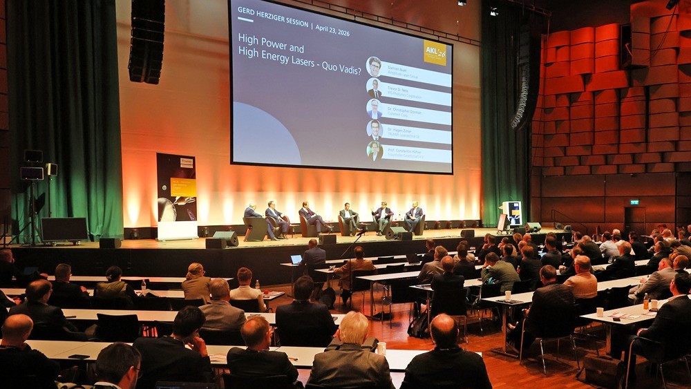
The International Laser Technology Congress has now served the sector for three decades. From April 22 to 24, AKL’26 brought together 544 experts from 21 countries, around 90 speakers and 57 exhibiting companies and institutions. In the Gerd Herziger Session, speakers reviewed how laser technology has moved from specialized applications into industrial infrastructure.
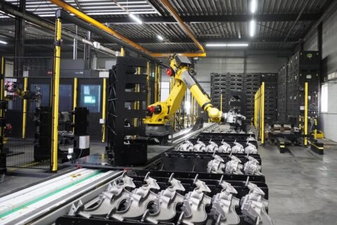
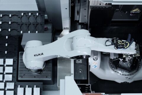
That shift is visible across many markets. Lasers are used in telecommunications, diagnostics and therapy, electric vehicle production, smartphone manufacturing, semiconductor processes, surface functionalization and material processing such as cutting, drilling, welding and soldering. New fields are also emerging, including fusion, quantum technology, agriculture, mining, offshore and underwater work, humanoid robotics and drone defense. The central message from the session was that the laser itself is increasingly only part of the story. Its value depends on integration, reliability, sensor technology, software and the ability to solve a specific production or inspection task.
Data centers create new demand for laser processes
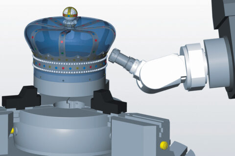
The rapid growth of data centers, much of it driven by artificial intelligence, is creating additional demand for laser-based manufacturing steps. Dr. Hagen Zimer, CEO of Laser Technology and member of the Executive Board of TRUMPF SE + Co. KG, pointed to a broad range of processes needed for AI chips, cooling systems, connections such as CPU parallel connections, hole drilling and cutting the sheet metal used in data center construction.
This demand reaches far beyond EUV lithography, although that remains one of the most demanding examples of industrial laser use. TRUMPF supplies laser technology to ASML for the next generation of AI chips, where structures are expected to reach feature sizes of 2 nanometers. The development path illustrates the long time horizon behind such breakthroughs. TRUMPF, ZEISS, Fraunhofer IOF in Jena, ASML and other partners worked for 15 years on this key technology for microchip manufacturing.
For production professionals, the lesson is not only that lasers enable smaller structures. It is that complex industrial progress often depends on stable supplier networks, long development cycles and a clear demand signal from system integrators and end users.
Shorter wavelengths improve semiconductor inspection
Dr. Christopher Dorman OBE, Executive Vice President Industrial at Coherent in Europe, described how inspection requirements in microelectronics have pushed laser technology toward shorter wavelengths. Around 20 years ago, wafers were inspected using green wavelengths around 500 nm. Today, 266 nm is used, and even shorter wavelengths are expected for faster and more accurate inspection.
The scale of the task is extreme. Inspecting a 300 mm wafer with nanometer-scale structures in process was compared to scanning Manhattan in twenty seconds, finding a single ant and identifying its species. This image captures the practical challenge facing semiconductor producers: inspection must become faster without missing defects that can affect yield.
Dorman also pointed to broader industrial progress. In cutting, the move from CO₂ lasers to fiber lasers has increased speeds from 15 cm per minute to 9 m per minute. The improvement is linked to higher power, shorter pulse durations and more flexible wavelengths. Similar trends are visible in flow cytometry. With two lasers, systems can count and analyze 10,000 cells per second. With nine wavelengths, that figure can rise to 150,000 cells per second, which matters when individual cells must be detected for diagnoses such as leukemia.
Fiber lasers expand into more production tasks
Trevor Ness, Senior Vice President and Chief Revenue Officer at IPG Photonics, described a future in which lasers are so widely integrated that users rarely think about them as separate technologies. His view reflects a broader industrial trend: fiber lasers have become more capable and reliable as semiconductor lasers have improved.
According to Ness, advances in diode lasers are keeping pace with Moore’s Law. This has supported strong growth in the laser industry and productivity gains for users in marking, cutting and welding. The same technology base is now moving into cleaning, drying and heat treatment. For manufacturers, this matters because a laser source can become part of a broader process platform rather than a single-purpose tool.
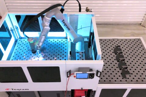
Power levels are also changing what is practical on the shop floor. Ness noted that lasers above 60 kW, including associated optics, are now manufactured routinely. In cutting, such systems are opening areas previously served by technologies such as plasma cutting. Optimized cutting heads and sensor technology have also made it possible to cut highly reflective metals such as aluminum, copper and brass more routinely with fiber lasers. Falling cost per watt is also supporting wider use, including handheld welding devices.
Applications take priority over the laser source
Several speakers argued that differentiation is shifting away from the laser source itself and toward the complete application. For users, the decisive factors are the function delivered, the price, reliability and service. Zimer emphasized that future systems will depend on beam guidance, sensor technology, digitalization, AI and stored process data.
That has direct implications for industrial adoption. A laser process is only valuable if it can be controlled, monitored and integrated into production with manageable effort. AI-supported process control is therefore becoming more relevant, particularly where materials, geometries or operating conditions vary. Better monitoring can also improve process stability and reduce the dependence on operator experience.
Ness described the laser of the future as intelligent, AI-capable, mobile on robot platforms, scalable and available in large quantities. One example is integration into humanoid robots. In such systems, the laser becomes a tool that allows robots to work in dangerous, confined or inaccessible environments, including nuclear facilities, deep sea operations, space or toxic surroundings. This raises technical opportunities and ethical questions, especially where directed energy is involved. The same applies to defense applications, where photonics companies see growth potential but must address the consequences of use.
Fusion could reshape photonics supply chains
Fusion was one of the most discussed future markets at AKL’26, although the speakers differed in their level of optimism. Zimer stressed that major investments need a solid business model. He noted that developing 2 kJ lasers for fusion power plants could require at least 100 to 200 million euros. Without concrete orders, supply chains and a clear customer, such development becomes difficult.
Damian Buet, CEO of Amplitude Laser Group, was more optimistic. His company develops femtosecond lasers for medical and industrial applications as well as high-energy large-scale lasers with peak powers of up to 3 petawatts. He acknowledged that today’s high-energy lasers are not yet designed for efficiency or continuous 10 to 20 Hz operation in power plants. However, he argued that technological challenges can be overcome if market demand is strong enough.
Fraunhofer ILT acting director Dr. Jochen Stollenwerk described the requirements for future fusion drivers: pulses in the multi-megajoule range, high repetition rates, efficiency of 10 to 20 percent and lifetimes of many billions of shots. Achieving this will require progress in gain media, cooling, optics and system architecture. It also demands that target fabrication, high-power target injection, optics, fuel cycles, chamber systems and plant operation mature in parallel.
Germany links fusion research to industrialization
Prof. Constantin Häfner, now responsible for research and technology transfer on the Executive Board of the Fraunhofer Society, outlined how Germany is positioning fusion as a central research topic. Shortly before AKL’26, the Federal Ministry of Research, Technology and Space announced that the research budget would rise to 3 billion euros before the end of the legislative term. Over the next eight to ten years, a budget of 8 billion euros is conceivable.
According to Häfner, funding will focus on three pillars. In magnetic fusion, Germany is backing a scaled stellarator rather than a tokamak design. In laser fusion, the country intends to build on strengths in optics and photonics. The third pillar concerns materials, including breeding tritium from lithium in power plants.
The planned fusion hubs are intended to connect supply chains from industry and research. Participants may include fusion startups, technology integrators, large industrial companies, energy suppliers, venture capital firms and international partners. The aim is to translate a fusion roadmap into detailed industrial roadmaps for the components needed for a power plant in the 2040s. For photonics suppliers, this could create demand for lasers, optics, materials and other components at a scale that drives down costs and opens adjacent markets, including secondary radiation sources and directed energy systems.