The rapid growth of the semiconductor market is creating new opportunities for grinding technology. With annual growth rates expected to exceed 30 percent, demand for high precision manufacturing processes is increasing sharply. At GrindingHub 2026 in Stuttgart, industry players demonstrated how grinding solutions are evolving to meet the requirements of wafer production, where surface quality and process efficiency are critical.
Semiconductors have become indispensable across a wide range of applications, from electric vehicles and charging infrastructure to renewable energy systems and communication technologies. This growing demand is placing pressure on manufacturing capacity and process speed. For Europe, which aims to strengthen its position relative to Asia and the United States, accelerating production processes is becoming a strategic priority.
From crystal growth to wafer precision
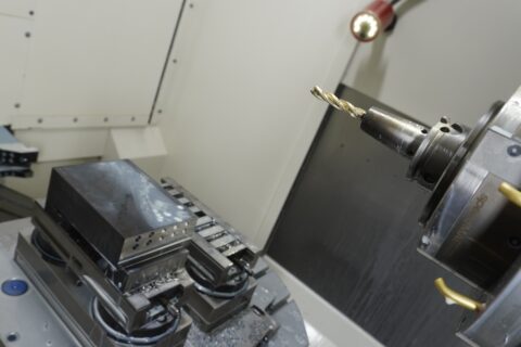
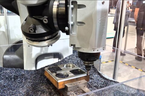
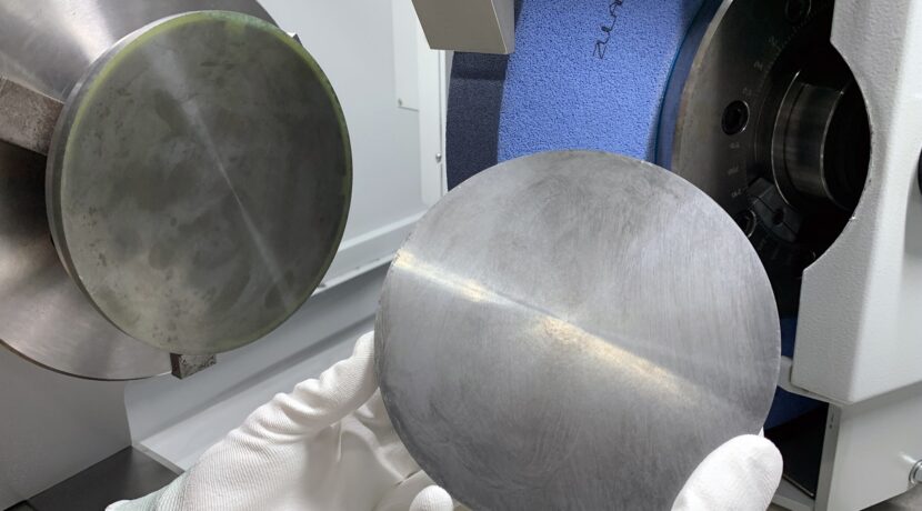
Wafer production consists of multiple process steps, each requiring a high degree of control. The process begins with the growth of single crystals, typically silicon or increasingly silicon carbide. These crystals are formed into ingots or boules, which are then processed into a preliminary shape known as a puck. The material is subsequently sliced into wafers, which undergo grinding, polishing and epitaxial coating before entering photolithography, where circuit patterns are created. The final step involves separating individual chips from the wafer.
According to Michael Egeter, Vice President Engineering at Kellenberger, the semiconductor sector offers significant growth potential for grinding technology suppliers. Opportunities exist not only in substrate preparation, such as pre-grinding and cutting raw crystals, but also in the broader field of semiconductor processing equipment. He emphasizes that machine builders can strengthen their position by developing application-specific solutions. Kellenberger has established dedicated teams focused on customization, with the aim of delivering scalable solutions tailored to individual customer requirements.
Silicon carbide drives new requirements
A key material trend is the increasing use of silicon carbide. Compared to conventional silicon, silicon carbide offers a wider band gap, which allows semiconductors to operate under higher temperatures, voltages and frequencies. This makes it particularly relevant for power electronics and demanding applications.
However, the material also introduces new challenges for grinding. Its ceramic nature differs fundamentally from metallic materials, requiring different process strategies and tooling approaches. According to Egeter, some grinding specialists initially show reluctance when transitioning to these materials. Once this barrier is overcome, the potential becomes clear. Silicon carbide has already established itself as a benchmark material for specific semiconductor performance classes, and its adoption is expected to continue growing.
At the same time, reducing lead times in semiconductor production is becoming increasingly important. The production of a raw crystal alone can take around two weeks, as it is grown in furnaces at temperatures of approximately 2,400 degrees Celsius. Subsequent processing steps further extend the overall production time.
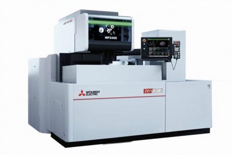
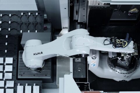
To address these inefficiencies, a development team within the Hardinge Group, including Kellenberger, has focused on optimizing the transition from ingot or boule to puck. The result is an automated 5-axis machine capable of processing all relevant silicon carbide ingot specifications and diameters. With automated loading and unloading, the system reduces processing time from more than 24 hours using conventional methods to between two and three hours.
Tooling defines surface quality
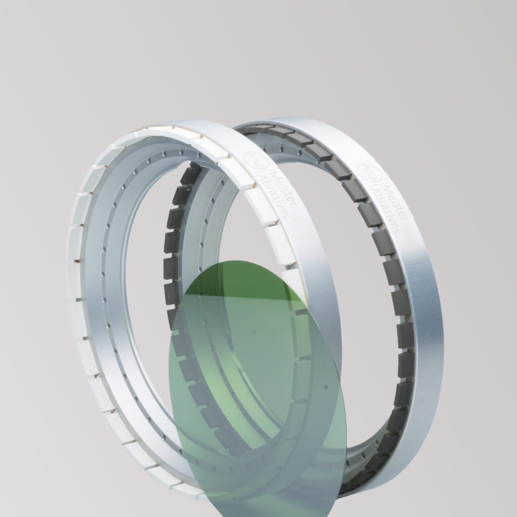
In addition to machines and materials, grinding tools play a critical role in wafer production. Carmine Sileno, Product Manager Semiconductor at Meister Abrasives, identifies the sector as a rapidly growing market for high precision tooling. The company develops superabrasive tools designed for the entire semiconductor value chain, from raw crystal to finished wafer.
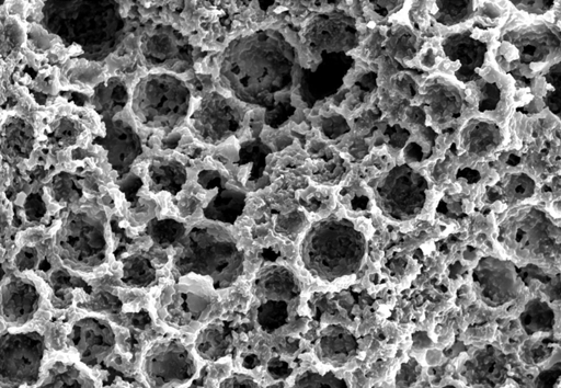
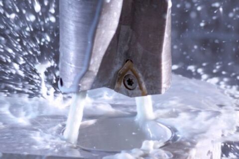
Diamond grinding tools are used to achieve extremely fine surface finishes, with roughness values in the range of Ra 5 angstrom. At this scale, conventional measurement methods are no longer sufficient. Quality assurance requires advanced techniques such as white light interferometry or atomic force microscopy.
Surface quality is not only defined by roughness but also by uniform nanotopography. Homogeneous surfaces are essential for subsequent process steps and overall chip performance. Meister Abrasives focuses on developing ultra-fine grinding solutions that reduce the need for additional finishing processes.
This approach is particularly relevant in the context of polishing. Traditionally, wafers are ground and then polished using slurries consisting of fine particles in a liquid medium. These processes are both time-consuming and costly. By improving grinding precision, it becomes possible to shorten or even eliminate polishing steps. This requires the development of suitable bonding systems for submicron diamond grains, an area where tool manufacturers are focusing their efforts.
Reducing or eliminating polishing not only lowers process costs but also simplifies infrastructure requirements and increases throughput. For semiconductor manufacturers, this translates into shorter production cycles and improved efficiency.
The European Union aims to increase its share of global semiconductor production from the current 9 to 10 percent in the coming years. Within this context, grinding technology suppliers see opportunities to expand their role, particularly by offering customized solutions in a market currently dominated by a limited number of global players.